
 Tiếng
Việt
Tiếng
Việt
 Tiếng
Anh
Tiếng
Anh
 Tiếng
Nhật
Tiếng
Nhật




 Tiếng Anh


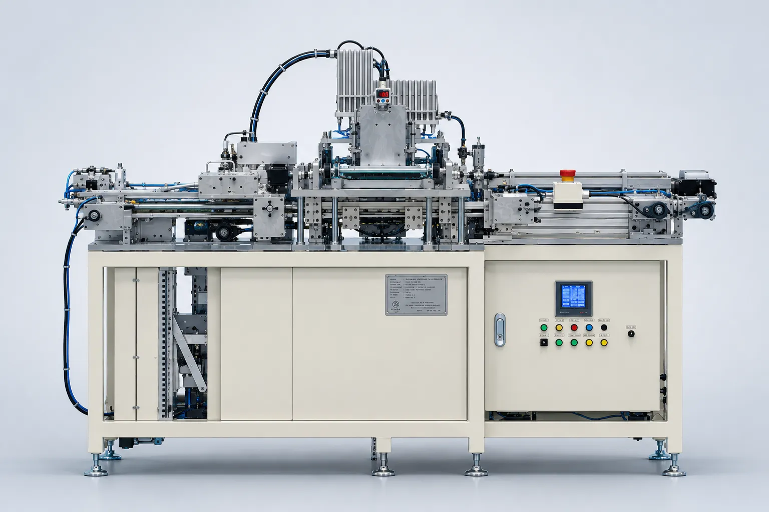
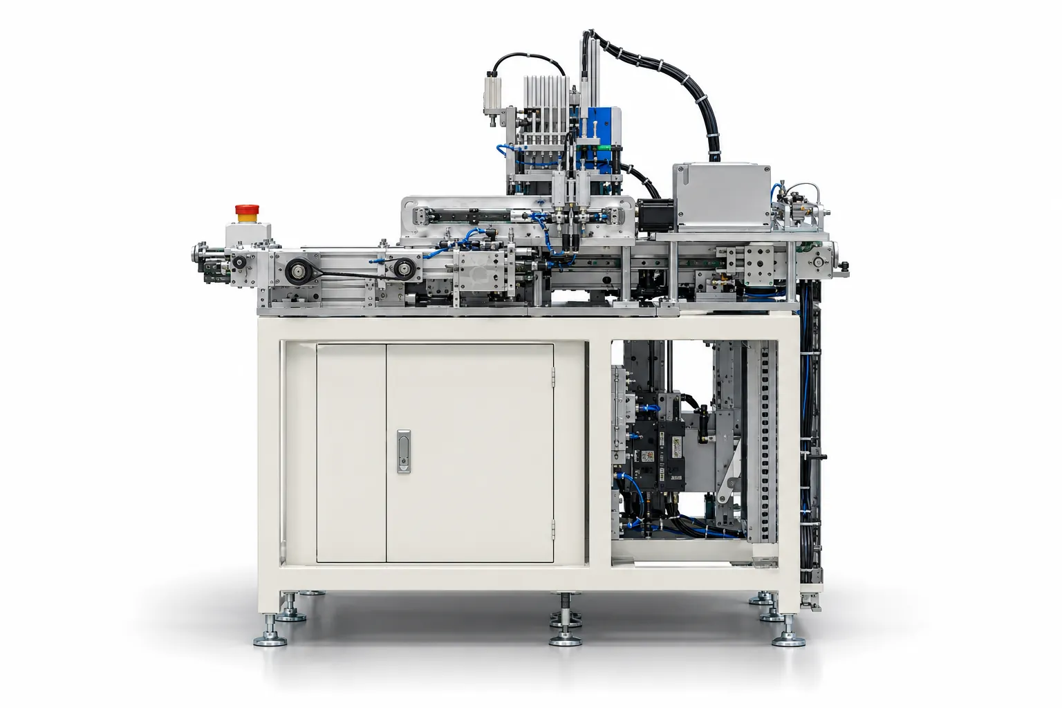
Machine for attaching electronic components
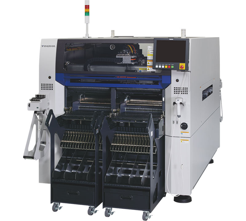
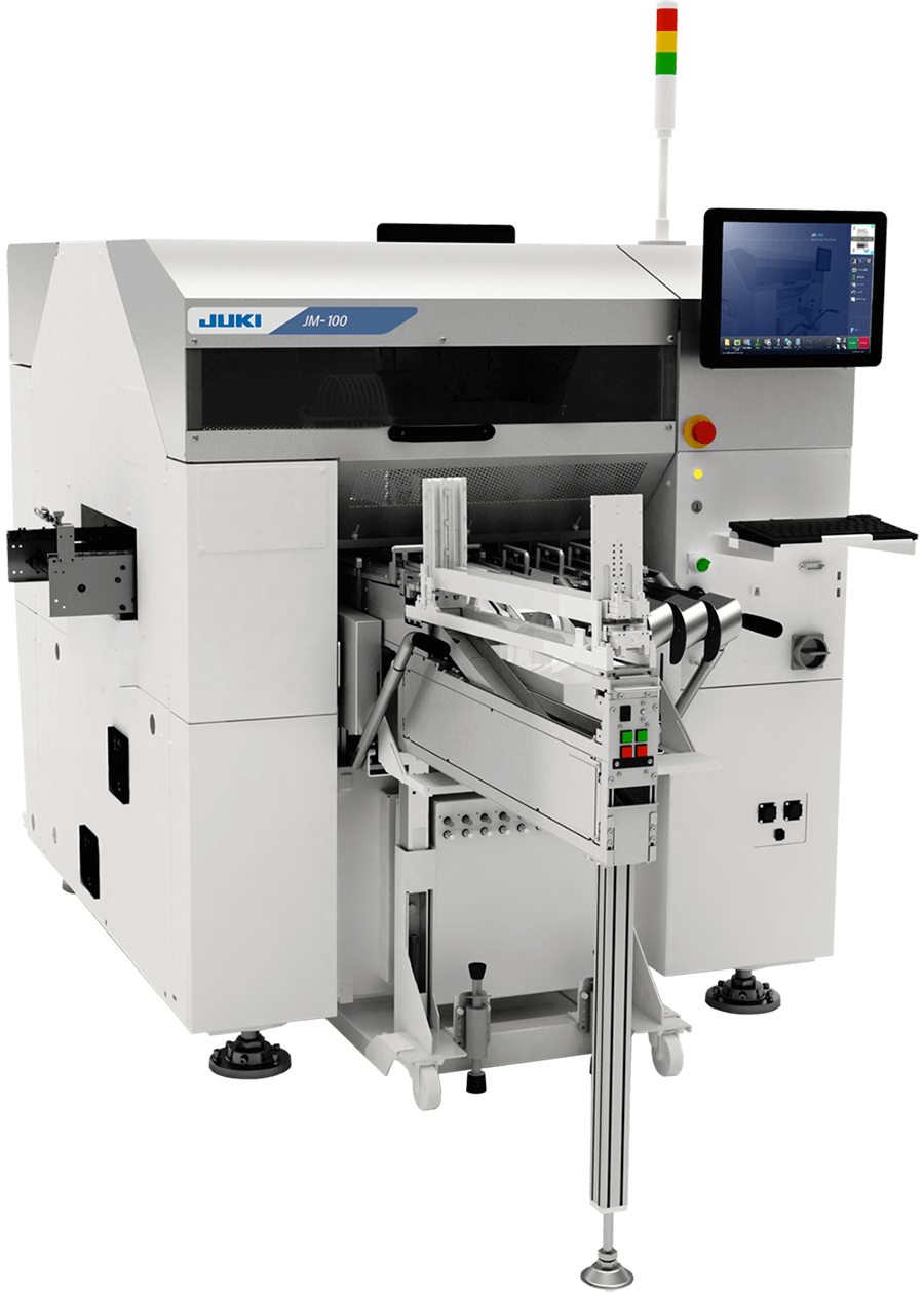
The electronic component placement machine is an automated solution used in PCB manufacturing, particularly in SMT (Surface Mount Technology), to accurately pick and place electronic components onto programmed positions on the PCB. Compared with manual assembly, the machine can continuously handle a wide range of SMD components, including resistors, capacitors, diodes, ICs, and other miniature components, while maintaining high placement speed and consistent accuracy.
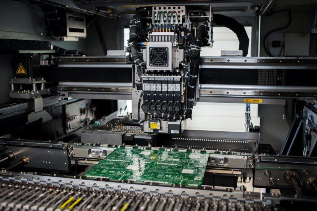
During operation, components are supplied through feeders or trays, then picked up by the placement head and accurately positioned onto the PCB. An integrated vision system and precision positioning mechanism identify the component and automatically correct its position and orientation before placement, helping minimize defects such as misalignment, incorrect orientation, and missing components. This automated process enables manufacturers to increase productivity, reduce dependence on manual labor, and maintain consistent assembly quality across production batches.
Depending on product specifications and production volume, the machine can be configured with different placement speeds, numbers of placement heads, component size ranges, and positioning accuracy. It can also be integrated with other SMT equipment, including solder paste printers, SPI inspection systems, reflow ovens, and AOI inspection machines, to create a continuous and highly automated PCB assembly line with improved process control and production efficiency.
VIETNAM CNC & TECHNOLOGY APPLICATION JOINT STOCK COMPANY
Hotline: +84.916 63 9355 / +84.915 74 4664
Email: Sales01@cncvina.com.vn / Sales03@cncvina.com.vn
Product description

Introduction to the Electronic Component Placement Machine
The electronic component placement machine is an automated solution used in PCB manufacturing, particularly in SMT (Surface Mount Technology), to accurately pick and place electronic components onto programmed positions on the PCB. Compared with manual assembly, the machine can continuously handle a wide range of SMD components, including resistors, capacitors, diodes, ICs, and other miniature components, while maintaining high placement speed and consistent accuracy. During operation, components are supplied through feeders or trays, then picked up by the placement head and accurately positioned onto the PCB. An integrated vision system and precision positioning mechanism identify the component and automatically correct its position and orientation before placement, helping minimize defects such as misalignment, incorrect orientation, and missing components. This automated process enables manufacturers to increase productivity, reduce dependence on manual labor, and maintain consistent assembly quality across production batches.
Depending on product specifications and production volume, the machine can be configured with different placement speeds, numbers of placement heads, component size ranges, and positioning accuracy. It can also be integrated with other SMT equipment, including solder paste printers, SPI inspection systems, reflow ovens, and AOI inspection machines, to create a continuous and highly automated PCB assembly line with improved process control and production efficiency.
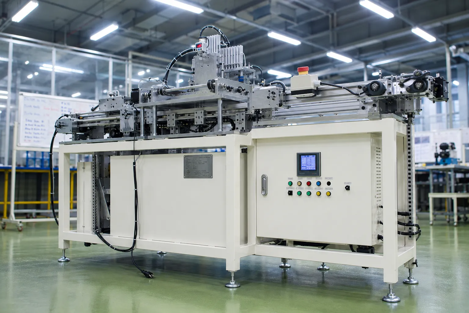
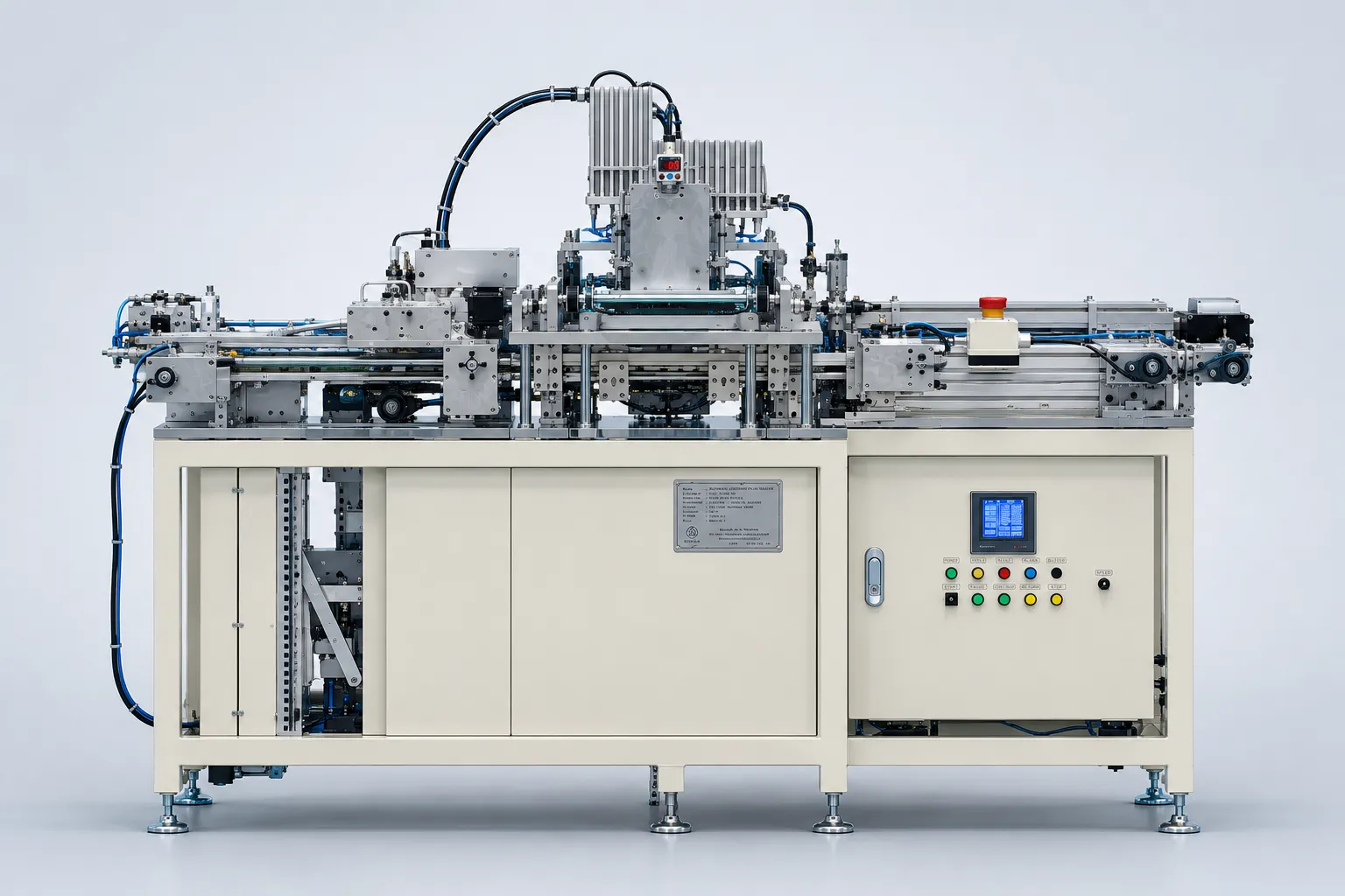
| Specification | Details |
|---|---|
| Machine Dimensions | W1120 × L1115 × H1235 mm |
| Power Supply | AC 220V, DC 10V |
| Average Operating Power | 1400 W |
| Air Pressure | 0.4–0.6 MPa |
| Maximum PCB Size | 400 × 350 mm |
| Machine Weight | 370 kg |
| Number of Placement Heads | 2–6 heads (customizable) |
| Placement Accuracy | ±0.05 mm |
| PCB Size | 400 × 350 mm |
Types of Electronic Component Placement Machines
Surface-Mount Device (SMD) Placement Equipment
Definition of SMT
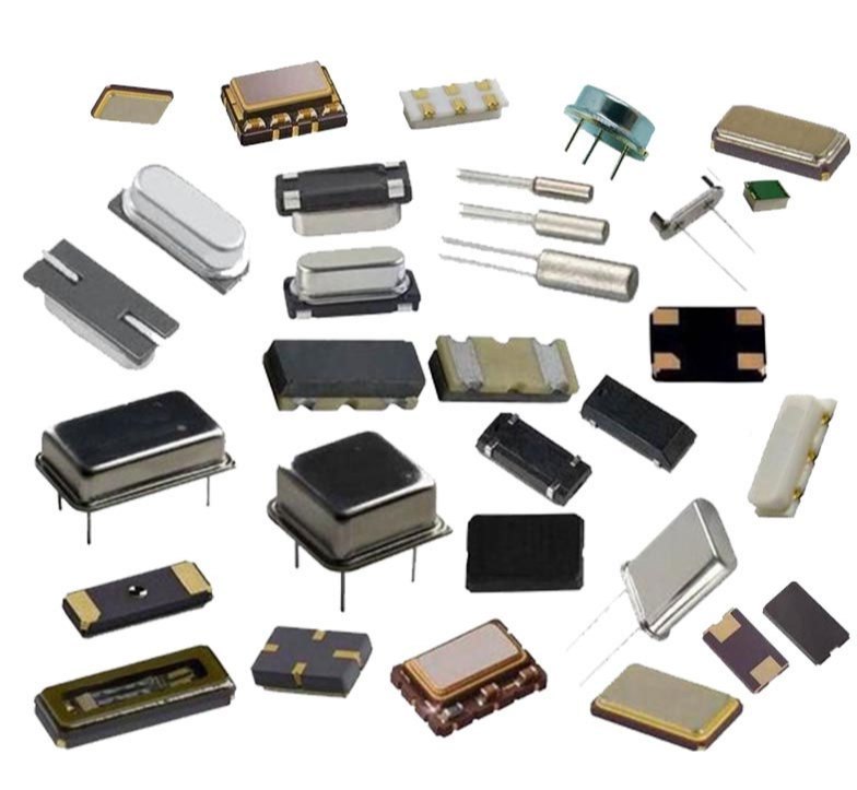
Surface Mount Technology (SMT) is an electronic assembly technology in which electronic components, commonly referred to as Surface-Mount Devices (SMDs), are mounted directly onto the surface of a printed circuit board (PCB).
Due to its high production efficiency, compact component layout, consistent assembly quality, and cost-effectiveness, SMT has become one of the most widely adopted technologies in modern electronics manufacturing. SMT placement equipment plays a key role in this process by automatically positioning and mounting components onto programmed locations on the PCB with high speed and precision.
Surface-Mount Resistor Networks
SMD resistor networks integrate multiple resistive elements into a single component, replacing multiple discrete resistors on a PCB. This design helps save valuable board space while reducing the number of components that need to be supplied and placed during the assembly process. Depending on the package design, resistor networks are available with different pin counts and resistance values to meet the requirements of control circuits, signal circuits, and various electronic devices. When used in an SMT production line, resistor network components can be automatically fed and placed in the same manner as other SMD components, helping improve production throughput and assembly consistency.
SMD Resistors
SMD resistors are among the most widely used components on electronic circuit boards. They typically feature a rectangular body with two electrodes at each end, allowing Pick-and-Place machines to accurately identify, pick, and place them at designated positions on the PCB. Common SMD resistors are manufactured using thick-film or thin-film technologies. Thick-film resistors typically use a resistive material deposited onto an alumina ceramic substrate, while thin-film resistors use a precision resistive film formed on a ceramic substrate. Differences in materials and manufacturing technologies enable these components to meet a wide range of requirements for resistance value, accuracy, thermal stability, and frequency characteristics.
For automated SMT production lines, the uniform size and shape of SMD resistors are important factors because they directly affect component feeding, recognition, and placement accuracy. Selecting the appropriate feeder, suction nozzle, and machine parameters helps minimize pick-up errors, placement offsets, and component drops during production.
SMD Tantalum Capacitors
SMD tantalum capacitors use tantalum as the electrode material and are commonly selected when high capacitance is required within a relatively compact package. With high capacitance per unit volume, tantalum capacitors are well suited for circuit designs where PCB space is limited. A key consideration when assembling tantalum capacitors is polarity. Unlike certain non-polarized ceramic capacitors, tantalum capacitors must be installed in the correct orientation. Therefore, the SMT system must accurately identify the component orientation before placement to prevent polarity-related assembly defects.
SMD tantalum capacitors are available in various package sizes and capacitance values and are widely used in power supply circuits, filtering applications, and electronic systems requiring stable electrical performance. For automated production, the feeding method and machine parameters should be configured according to the component dimensions, package shape, and orientation requirements.
SMD Ceramic Capacitors
Multilayer Ceramic Capacitors (MLCCs) are among the most widely used SMD components in modern electronics manufacturing. Their compact, leadless structure enables efficient PCB utilization, while their electrical characteristics make them suitable for a wide range of frequency applications, particularly noise filtering, signal coupling, and power supply decoupling.
MLCCs are available in various package sizes and capacitance values. Smaller packages allow manufacturers to achieve higher component density on the PCB, while larger packages can provide higher capacitance or meet specific electrical requirements.
Because MLCCs can be extremely small, their feeding and placement require highly accurate SMT equipment. Component feeders, Pick-and-Place machines, and post-placement inspection systems must be properly configured to minimize missing components, placement offsets, and component damage during production.
Active SMD Components
Unlike passive components, active SMD components are capable of performing functions such as signal amplification, processing, control, and electrical switching. This category includes a wide range of package types, where package dimensions, pin count, lead pitch, and connection structure directly influence SMT assembly requirements.
PLCC – Plastic Leaded Chip Carrier
PLCC (Plastic Leaded Chip Carrier) is an SMD package featuring connection leads arranged around the edges of the package and formed into a J-shaped configuration. This structure provides a certain degree of mechanical compliance, helping absorb mechanical stress and reduce direct stress on solder joints when the PCB experiences deformation or thermal expansion. PLCC packages offer relatively compact dimensions and efficient PCB space utilization, while also being compatible with automated SMT assembly systems. However, the polymer material used in the package can absorb moisture, so proper storage and handling are required before the components are introduced into the production line. Moisture control is particularly important during heating and reflow soldering, as moisture accumulated inside the package may expand and affect component reliability.
Fine-Pitch SMD Packages
Fine-pitch is a general term used for SMD packages with very small spacing between adjacent leads or terminals. The reduced lead pitch allows a large number of electrical connections to be integrated within a compact package, supporting the ongoing trend toward smaller electronic devices and higher functional density.
However, smaller lead pitch also places higher demands on the assembly process. The PCB must be designed with an appropriate land pattern, while the solder paste printer, Pick-and-Place machine, and inspection systems must provide the required level of precision. Even minor deviations during solder paste printing or component placement can result in defects such as solder bridging, insufficient solder, or component misalignment. Therefore, when selecting equipment for an SMT line using fine-pitch components, manufacturers should consider positioning accuracy, component recognition capability, vision systems, and the machine's ability to handle fine-pitch packages.
SOIC – Small Outline Integrated Circuit
SOIC (Small Outline Integrated Circuit) is a widely used SMD IC package with leads arranged along both sides of the package body. The leads are typically formed in a gull-wing configuration, providing favorable conditions for soldering and visual inspection. SOIC packages are available in various pin counts, package dimensions, and lead pitches, making them suitable for applications ranging from control circuits and signal processing to industrial electronic equipment. Compared with packages featuring finer pitches, SOIC packages are relatively easy to handle during automated placement and inspection. In an SMT production line, accurate recognition of the IC's shape, position, and orientation is essential. The Pick-and-Place machine must accurately determine the component center and rotation angle before placement to ensure that the IC leads align correctly with the PCB pads.
SOJ – Small Outline J-Lead
SOJ (Small Outline J-Lead) is an SMD package featuring J-shaped leads arranged along both sides of the package body. This structure combines the space-saving advantages of a small-outline package with the mechanical characteristics of J-lead connections. SOJ packages were widely used in memory devices such as DRAM and in certain specialized integrated circuits. Although many modern electronic designs have transitioned to higher-density package technologies, SOJ remains an important package type in the development and evolution of SMD packaging technology.
Through-Hole Technology (THT)
Definition of THT
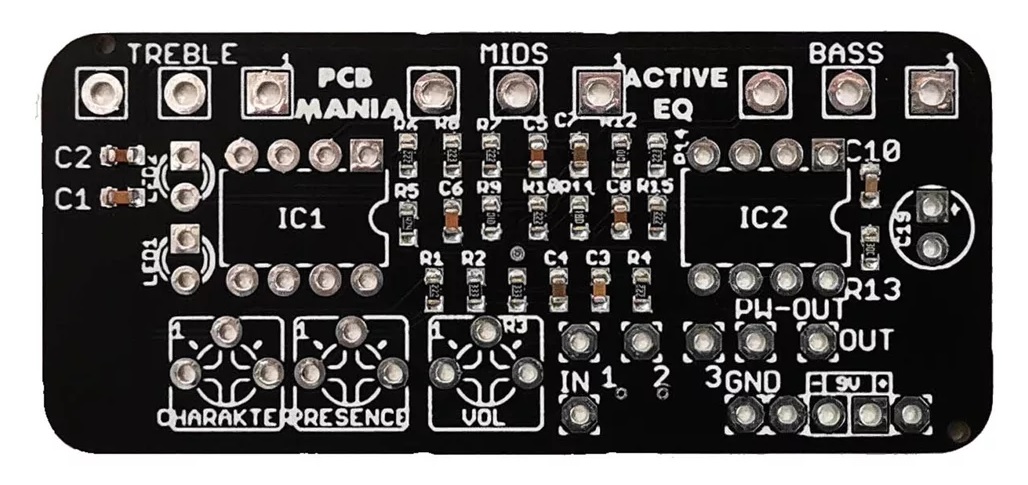
Through-Hole Technology (THT) is an electronic assembly method in which component leads are inserted through drilled holes in a printed circuit board (PCB) and soldered to pads on the opposite side of the board.
The THT process typically involves drilling holes in the PCB, inserting the component leads through the designated holes, and then soldering the leads to the corresponding pads. This process creates a strong mechanical and electrical connection between the component and the PCB.
Due to its robust connection structure and high mechanical strength, THT remains an ideal solution for applications requiring high reliability, durability, and resistance to mechanical stress. It is commonly used for components such as connectors, transformers, large capacitors, switches, and other components that require a strong physical connection to the PCB.
Advantages of Through-Hole Technology (THT)
One of the key advantages of Through-Hole Technology (THT) is its ability to accommodate high-power components, making it particularly suitable for power electronics applications. THT components also offer excellent resistance to high temperatures and mechanical vibration, making them well suited for demanding industrial environments. In addition, the THT assembly process is relatively straightforward, providing manufacturers with a practical and cost-effective solution for applications requiring robust component connections.
Through-Hole Technology offers several advantages in electronic manufacturing, including:
High Mechanical Strength: THT creates a strong and durable mechanical and electrical connection between components and the PCB, making it suitable for applications requiring high reliability and long-term durability.
High-Power Handling: THT is well suited for high-power components and is therefore widely used in power electronics and applications involving high current or voltage levels.
Resistance to Harsh Environments: THT components can withstand elevated temperatures, mechanical vibration, and other demanding operating conditions, making them suitable for industrial and harsh-environment applications.
Cost-Effective Assembly: The THT process is relatively straightforward and can provide a cost-effective assembly solution for specific PCB applications, particularly where component quantity and placement complexity are limited.
Easy Maintenance and Repair: THT components can generally be removed and replaced more easily than many densely packed SMD components, simplifying maintenance, troubleshooting, and repair operations.
High Reliability: The robust connection created by through-hole soldering helps reduce the risk of component detachment and mechanical failure, contributing to the long-term reliability of the finished electronic product.
Long-Term Component Availability: Certain THT components are available with longer product life cycles and remain widely used in industrial equipment, power electronics, and specialized applications where long-term reliability and maintenance are important considerations.
Hybrid Assembly
Definition of Hybrid PCB Assembly
Hybrid PCB assembly combines multiple electronic assembly technologies, including Surface Mount Technology (SMT), Through-Hole Technology (THT), and Ball Grid Array (BGA) packaging, within the same PCB assembly.
In other words, hybrid assembly integrates Surface-Mount Devices (SMDs), through-hole components, and BGA packages to take advantage of the specific benefits offered by each technology. This approach is commonly applied to complex electronic products where different types of components and connection methods are required on the same PCB.
Hybrid PCB assembly provides greater flexibility in component selection and board design, allowing manufacturers to use compact SMD components for high-density areas, THT components where strong mechanical connections are required, and BGA packages where a high number of electrical connections must be accommodated within a limited PCB area.
For automated production, hybrid assembly can be implemented by integrating multiple processes and dedicated equipment into a coordinated production line. This enables manufacturers to optimize placement accuracy, soldering quality, production efficiency, and overall process control according to the specific requirements of each PCB design.
Advantages of Hybrid PCB Assembly
Hybrid PCB assembly is a relatively advanced approach in modern electronics manufacturing, combining the advantages of multiple assembly technologies to accommodate different component types and application requirements. Key advantages include:
- Support for multiple component types: Hybrid assembly can accommodate through-hole (THT), surface-mount (SMT), and BGA components on the same PCB.
- Flexible single- and double-sided assembly: Supports single-sided or double-sided SMT and BGA assembly, including Micro-BGA applications.
- 100% X-ray inspection: X-ray inspection can be applied to verify hidden solder joints, particularly for BGA and other high-density components, facilitating quality control and rework.
- Wide range of component compatibility: Suitable for advanced PCB components such as BGA, QFN, CSP, 0201, 01005, PoP, and small-batch press-fit components.
- Polarized component support: Compatible with both polarized SMT components and polarized through-hole components.
- Advanced rework capability: Supports the removal and replacement of BGA and MBGA components, including ceramic and plastic BGA packages, as well as BGA and MBGA reballing processes.
- RF and digital integration: Enables RF and digital electronic circuits to be integrated on a single PCB, providing greater design flexibility.
- Compact and lightweight design: Helps reduce the overall size and weight of electronic assemblies while minimizing or eliminating unnecessary cables and wiring harnesses.
- High reliability: Combines the precision of SMT with the robust mechanical connections of THT, improving the overall reliability of the finished product.
- Cost efficiency: Optimizes manufacturing processes by allowing different assembly technologies to be applied according to the specific requirements of each component.
- High precision and automation: Maintains the high placement accuracy and automated production capabilities of SMT while retaining the mechanical strength of THT connections.
Although SMD components are widely used in modern PCB manufacturing, certain components are not suitable for SMT assembly. For this reason, combining SMT and THT technologies on the same PCB is often the most effective solution. This hybrid approach provides the benefits of SMT, such as high placement accuracy, compact size, lightweight design, and easy automation, while retaining the advantages of THT, including strong mechanical connections and high resistance to mechanical and thermal stress.
SMT and THT also require different soldering processes. Surface-mount components are typically soldered using reflow soldering, while through-hole components are commonly assembled using wave soldering or selective/manual soldering, depending on the product design and production requirements.
Main Components of an Electronic Component Placement Machine
Feeding System
Definition of the SMT Feeding System
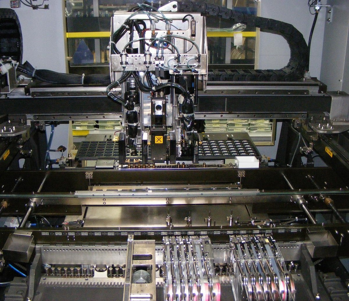
An SMT feeder, also known as a component feeder or part feeder, is a critical device used to supply SMD components from tape-and-reel packaging to the pick-and-place machine. The feeder secures the component tape, removes the protective cover tape, and advances the exposed components to a designated pick-up position, allowing the placement head to accurately pick and place each component onto the PCB.
The SMT feeder is one of the most important components of an SMT placement machine, as its feeding accuracy and stability directly affect PCB assembly quality, placement efficiency, and overall production performance.
Most SMD components are supplied on paper or plastic carrier tape wound into reels and loaded into feeders installed on the placement machine. Larger integrated circuits (ICs) may also be supplied in trays or sticks. However, advances in feeder technology have made tape-and-reel packaging one of the most widely used component supply methods in modern SMT production.
Types of SMT Feeders
Depending on the component packaging format, SMT feeders can generally be classified into tape feeders, tray feeders, stick feeders, and tube feeders.
Tape Feeder:
Tape feeders are the most commonly used feeding systems on SMT placement machines. Traditional designs include wheel-driven, claw-type, pneumatic, and electric mechanisms. Modern high-precision electric feeders provide faster feeding speeds, improved positioning accuracy, compact construction, and greater operational stability, helping increase overall production efficiency.
Tray Feeder:
Tray feeders are available in single-level and multi-level configurations. Single-level tray feeders are installed directly on the placement machine and are suitable for components supplied in a limited number of trays. Multi-level tray feeders feature automatic tray transfer and offer a compact solution for IC components such as TQFP, PQFP, BGA, TSOP, and SSOP packages.
Stick Feeder:
Stick feeders are designed to supply loose components packaged in plastic sticks or tubes. Components are continuously transferred to the pick-up position using vibration mechanisms or dedicated feeding channels. This method is commonly used for MELF and other small semiconductor components, particularly non-polarized rectangular or cylindrical components.
Tube Feeder:
Tube feeders typically use a vibration mechanism to continuously move components inside a tube toward the pick-up position. They are commonly used for components such as PLCC and SOIC packages. This feeding method provides good protection for component leads, although feeding stability and production efficiency may be lower compared with tape-based systems.
Placement System
The SMT component placement system, commonly known as a Pick-and-Place (P&P) machine, is a high-speed automated system designed to accurately place surface-mount devices (SMDs) onto printed circuit boards (PCBs).
The system is capable of handling a wide range of electronic components, including resistors, capacitors, ICs, and other semiconductor devices, making it an essential part of modern electronics manufacturing. It is widely used in consumer electronics, industrial equipment, medical devices, automotive electronics, telecommunications, and other applications requiring high-speed and high-precision PCB assembly. The placement system operates as part of a larger automated PCB assembly line. Multiple subsystems work together to pick components from feeders, accurately position and orient them, and place them at programmed coordinates on the PCB. High-precision motion mechanisms, servo drives, and vacuum nozzles enable accurate movement in multiple axes while maintaining stable and repeatable placement performance.
Vision System
Definition of the Vision System
The vision system is a key component of an SMT placement machine. It is responsible for identifying component position, orientation, and PCB reference points, directly contributing to the placement accuracy and operational efficiency of the machine.
Features of the Vision System
High-performance SMT machines typically utilize advanced image-processing technology to inspect and align components before placement. When a nozzle picks up a component, the vision system captures its image using a camera positioned on the placement head or at a designated location within the machine.
The captured image is processed digitally to determine the component's position, orientation, and other relevant characteristics. The image-processing system then compares the detected information with the programmed parameters and sends correction data to the machine controller. The servo system automatically compensates for positional or angular deviations before the component is placed onto the PCB.
This process enables the machine to accurately handle miniature chip components, fine-pitch ICs, and components with complex shapes while maintaining high placement speed and repeatability. The entire sequence—including component recognition, alignment, inspection, correction, and placement—is automatically controlled by the industrial PC and machine control system according to the programmed production parameters. The vision system can also communicate with the machine database, control system, and calibration system through the HMI or automated interfaces. Through the HMI, operators can perform functions such as real-time image acquisition, image display, inspection, and system configuration.
Vision System Challenges
The vision system of a component placement machine must address two major technical challenges.
The first is system integration, which involves LED lighting control, image acquisition, digital data transmission, image processing, and communication between the vision system and machine controller.
The second is image-processing algorithms, particularly those related to component recognition, orientation detection, positional correction, and high-speed image processing.
Advanced industrial cameras and image-processing hardware can be integrated into the placement machine to detect PCB reference points, automatically recognize components, correct positional deviations, and ensure accurate component placement. This vision system effectively functions as the machine's "eyes," enabling reliable and precise automated assembly.
Applications and Industries for Electronic Component Placement Machines
Electronic component placement machines are widely used in PCB manufacturing and SMT production lines. Instead of manually placing components onto the board, the automated system identifies PCB coordinates, picks components from the appropriate feeders, and places them accurately at programmed positions with high speed and repeatability. This enables manufacturers to achieve consistent assembly quality while maintaining stable production capacity, particularly in high-volume manufacturing environments. In practice, electronic component placement machines can be integrated into various stages of an SMT production line, including PCB loading, solder paste printing, component placement, reflow soldering, and post-assembly inspection.
Depending on the product and production requirements, manufacturers can select machines with different placement speeds, accuracy levels, numbers of placement heads, feeder configurations, and component-handling capabilities.
Advancements and Future Trends in Electronic Component Placement Machines
SMT manufacturing technology has continued to evolve since its widespread adoption in the electronics industry during the 1980s. Continuous improvements in component miniaturization, automation, materials, and machine technology are driving SMT production toward higher speed, greater precision, and improved manufacturing efficiency.
LED Technology
Light-emitting diode (LED) technology has become increasingly important in electronics manufacturing. LEDs offer advantages such as compact size, low power consumption, and long service life. When combined with high-speed SMT assembly technologies, LED production can benefit from faster manufacturing cycles, reduced labor requirements, and improved production efficiency.
Solder Paste Technology
Solder paste technology continues to play an important role in improving PCB assembly quality and efficiency. Recent developments include fine-particle solder pastes, water-soluble formulations, and no-clean solder pastes. These technologies help improve printing performance, solder joint quality, process stability, and production efficiency, particularly for increasingly compact electronic assemblies.
Increasing SMT Placement Speed and Precision
Modern electronics manufacturers face increasing demand for smaller, lighter, and more powerful products. SMT technology enables manufacturers to place increasingly miniature components onto compact PCBs while maintaining high placement accuracy. As component sizes continue to decrease and advanced solder materials and inspection technologies become more widely adopted, manufacturers can integrate more components into smaller PCB designs. This enables electronics companies to develop compact and lightweight products while maintaining increasingly sophisticated functionality. Higher levels of automation also help reduce production time, labor requirements, and human-related assembly errors. As a result, SMT technology will continue to play an important role in the development of modern electronics manufacturing.
Although different types of component placement equipment may vary in structure and function, they generally operate according to the same fundamental principle: automatically feeding, identifying, picking, positioning, and placing electronic components onto a PCB according to a programmed process. An electronic component placement machine is one of the key pieces of equipment in an SMT production line, enabling manufacturers to automate SMD component placement with high speed, stable accuracy, and reliable repeatability. From small resistors and capacitors to ICs, fine-pitch packages, and other advanced components, each component type has specific requirements for feeders, nozzles, vision recognition, and placement accuracy.
Therefore, when investing in a component placement machine, manufacturers should consider more than simply the placement speed. Key factors include PCB dimensions, component types and sizes, required placement accuracy, number of placement heads, feeder compatibility, and integration capability with other SMT equipment. Selecting the appropriate machine configuration from the beginning can help manufacturers minimize assembly defects, optimize investment costs, improve production efficiency, and establish a solid foundation for future production expansion.
Customers who need Electronic Component Mounting Machines please contact:
VIETNAM CNC & TECHNOLOGY APPLICATION JOINT STOCK COMPANY
Factory: Song Cung Industrial Site, Dong Thap Commune, Dan Phuong District, City. Hanoi Vietnam
Phone: +84.916 63 9355 / +84.915 74 4664
Website: www.cncvina.com.vn ; www.cncvina.net
Email: Sales01@cncvina.com.vn / Sales03@cncvina.com.vn


